
Keynote Speakers
More Speakers to be Announced Soon
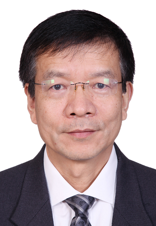
Hanming WU
Chairman of EtownIP Corporation, China
Hanming Wu earned PhD from Chinese Academy of Sciences in 1987, and post-doc in UC-Berkeley. More than 20 years industry experience in plasma application in semiconductor processes, including Novellus Systems, Intel Corp and SMIC. Along with 80 published papers, more than 42 granted and pending granted patents in semiconductor processes are to his credit. He has some experience of giving lectures at top universities in USA. Some of research results have been included in the textbook in USA.
Since 2001, he has joined and led the pre-study of technology development from 0.18um to 32nm node. As a director of Component Research with SMIC, he is now in charge of 32nm research program. Besides, he is a joined guest professor of Fudan University and Xi'An University of Electronics, Research Professor with Institute of Physics, member of technical board with Institute of Microelectronics, Chinese Academy of Sciences. In 2008, he earned the 2nd class award of National Science and Technology Progress.
Speech Title: Innovation of Integrated Circuit Manufacturing Industry Chain in More-than-Moore Era
Abstract: Today's integrated circuit industry has followed Moore's law for more than 60 years. Is the industry entering the post-Moore era? After analyzing the essence meaning of Moore's law, it can be considered that the industry has entered the post-Moore era. Thus, technology development faces many challenges and opportunities. From the perspective of innovation-driven development, it is necessary to lead the four models: manage technology R&D projects, business model, industry chain management and technology development. In the face of great opportunities, the need for the industry can not be targeted for immediate success blindly on the scale, and wild ambition for so-called corner overtaking opportunities. Industry should lay a solid emphasis on technology research and development on basic/foundamental research. Only in this way can we have the opportunity to carve out a development path with the unique characteristics. Moore's law may come to the end, whereas, innovation will go on and continue forever.
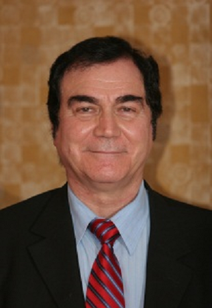
Paolo A. Gargini
IEEE Fellow and Former Intel Fellow , Italy
Dr. Gargini was born in Florence, Italy and received a doctorate in Electrical Engineering in 1970 and a doctorate in Physics in 1975 from the Università di Bologna, Italy, both with full honor and marks.
He has done research at Stanford University and at Fairchild Camera and Instrument (Research and Development) in Palo Alto in the early 70s.
Since joining Intel in 1978 he was responsible for Microprocessor technology including 80286 and the 80386 processors. In 1985 he headed the first submicron process development team at Intel. He was also responsible for all equipment selections from 1994 to 2007.
In 1996, Dr. Gargini was elevated to Director of Technology Strategy, Intel Fellow.
He was responsible for worldwide consortia research for the Technology and Manufacturing Group (TMG) from 1993 to 2012; he was member of Sematech, SRC and SIA Boards. Thorough the years Dr. Gargini successfully transferred the foundations of fundamental technologies into Intel such as: Copper interconnects, 248nm and 193nm lithography, Strained Silicon, High-K/Metal-Gate, FinFET and many new materials.
From 1998 to 2015, Dr. Gargini has been the Chairman of the International Technology Roadmap for Semiconductors (ITRS) sponsored by the WSC. Since 2016 he is the Chairman of the International Roadmap for Devices and Systems (IRDS) sponsored by IEEE.
Dr. Gargini became the first Chairman of the Governing Council of the Nanoelectronics Research Initiative (NRI) funded in June 2005 by SIA.
He is co-chairman of the EUVL Symposium.
Dr. Gargini was inducted in the VLSI Research Hall of Fame in 2009.
Dr. Gargini was elevated to IEEE Fellow in 2009 and to International Fellow of the Japan Society of Applied Physics in 2014.
Dr. Gargini is chairman of ETAB of E3S (UCB); he is also a member of NEREID Advisory Board (ETAB) for the European Roadmap.
He is a member of the leadership committee of the IEEE initiative on Future Networks aimed at 5G and Beyond Roadmap.
Speech Title: How to Successfully Overcome Inflection Points by using the Technology Roadmap Methodology
Abstract: “Geometrical Scaling” characterized the 70’s, 80’s and 90’s. The NTRS identified major transistors material and structural limitations. To solve these problems the ITRS introduced strained silicon, high-κ/metal gate, FinFET, and other semiconductor materials under “Equivalent Scaling”.
Horizontal (2D) features will reach a limit beyond 2020. Flash producers have adopted the vertical dimension. Logic producers will follow. IRDS assessed that “3D Power Scaling” will extend Moore’s Law for at least another 15 years. Furthermore, computing performance will be substantially improved by monolithically integrating several new heterogeneous memory layers on top of logic layers powered by a combination of CMOS and “new switch” transistors.
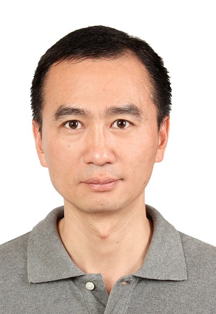
Liming Ge
Director, Wireless Hardware Development Unit, Huawei, China
Liming Ge has more than 20 years industry experience in wireless communication from 2G to 5G. He works in RF circuit design including transceiver and PA since joined Huawei in 1998. He has lead the power amplifier trend for many years in telecommunication. Now he is the director of wireless hardware development unit in Huawei, his work is focusing on the next generation platform for 5G base station.
Speech Title: The several trend discussions on RF integrated citcuit in 5G base station
Abstract: 5G is coming. As the main type of 5G base station, the massive MIMO is not easy to volume deployment because of several issues: the size is too big, the cost is too high and the performance cannot achieve the target in C band and millimeter wave. We already work a long time to solve it, but we still hope whole industry improve in different sides and let 5G can be acceptable by operators.

Jamie Schaeffer
Senior Director, Product Offering Management, GlobalFoundries,USA
Jamie Schaeffer is currently responsible for the FDX product offerings, including 22FDX and 12FDX, which enable differentiated solutions for the mobile, wireless networking, Internet of Things, and automotive markets. Prior to this, he had an extensive career in technology development at GlobalFoundries, Freescale Semiconductor, and the latter’s predecessor, Motorola Semiconductor Products Sector. He helped lead the development and transfer into volume manufacturing of the 32- and 28-nm technologies, and his earlier work in the semiconductor industry has been recognized with numerous invited talks and a Distinguished Innovator award for his contributions to technology innovation while at Freescale Semiconductor. He holds a bachelor’s degree in materials science and engineering from Cornell University and a Ph.D. degree in materials science and engineering from the University of Texas, Austin.
Speech Title: Optimizing the Leading Edge of Semiconductor Manufacturing
Abstract: Today's increasing rate of data consumption and intelligence at the edge, combined with the physical and economic challenges associated with the relentless pursuit of Moore’s law, is driving new vectors of semiconductor innovation. These vectors include a shift from general purpose to domain specific computing architectures and from “one size fits all” semiconductor technologies to application optimized semiconductor offerings. In this talk we will explore how the right combination of design architecture and leading edge process technology (FinFET, FDSOI, or RFSOI) is creating the next disruption in energy efficient computing, communication, and connectivity solutions.